Daniel Schulze, Engineering Manager at Dyconex02.07.20
Almost all markets are experiencing increasing demand for smaller and thinner electronic devices. Today’s mobile devices are small enough to fit in a watch, and the aerospace and automotive industries desire smaller and lighter devices to lower fuel costs and reduce emissions. Likewise, the medical industry needs wearable sensors, implantable devices, and handheld instruments that are small and lightweight.
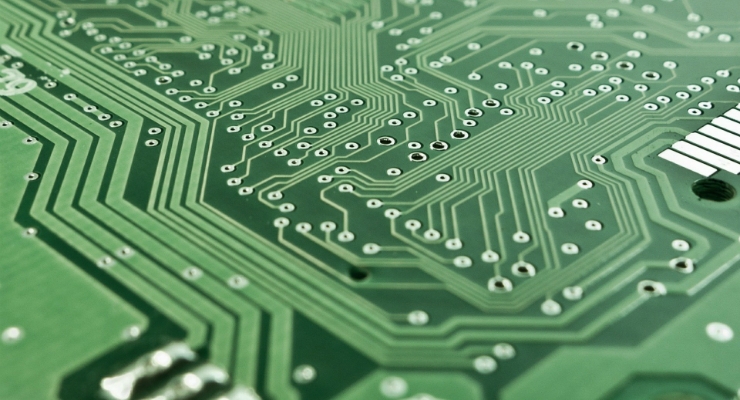
Manufacturers of the printed circuit boards (PCBs) that are at the heart of these electronic devices have been making them more compact and lighter primarily by decreasing the size of the copper features and board materials. Extremely thin base materials are making it possible to take miniaturization beyond what was previously possible without compromising reliability or performance.
Thinner Substrates
Although a great deal of miniaturization can be achieved in the X and Y directions, the technology is beginning to reach its limits. Another level of compactness is possible by using rigid and flexible ultra-thin base materials to make highly reliable PCBs that are thinner. While miniaturization in X / Y direction can greatly reduce the footprint of PCBs, miniaturization in the Z direction leaves more space for other components and reduces the overall thickness of the device.
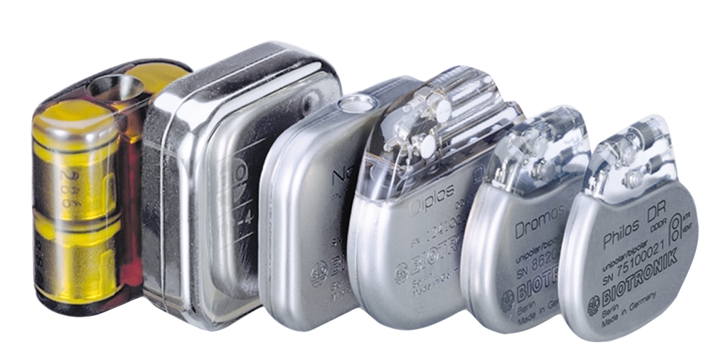
Figure 1. Evolution of pacemakers. Image courtesy of Dyconex.
With thinner base materials, less plated copper is needed to fill via connections. This automatically results in thinner copper layers and, therefore, lines/spaces with smaller resolutions and a reduced interconnect footprint.
Flex systems
Medical devices, like hearing aids and active implants, often require PCBs that can fit into the smallest area possible to improve the patients’ comfort. With flexible substrates, it is possible to create PCBs that fold to reduce the surface area and volume needed to house the PCB and thus increase the integration density. Using thinner flex materials rather than traditional thick flex materials can reduce the space needed for the PCB even more. For example, a six-layer flex system is about half the thickness of a system fabricated with standard flexible materials.
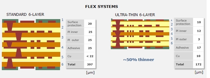
Figure 2. 6-layer stack-up with standard flex material compared to 6-layer stack-up with ultra-thin base material.
Flex systems are used in hearing aids to ensure all the necessary electrical components can be housed within a package that fits in the ear canal. In this case, the circuit board is assembled flat with the integrated circuits, resistors, and capacitors and then folded to reduce the overall footprint.
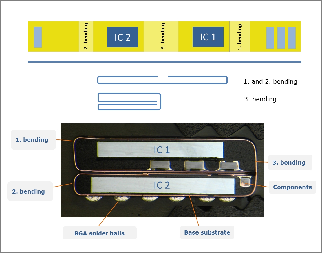
Figure 3. From flat substrate to folded package.
Ultra-thin flexible substrates also allow better bending. This means the PCBs can be bent with smaller bend radii to achieve even smaller volumes. A comparison is shown in Table 1. The improved bending makes ultra-thin flexible materials ideal for making cables that require dynamic bending, as in robotic arms.
Today, the outer layers of a multilayer flex system typically measure 12 µm for the polyimide and 12 µm for the adhesive. The new FRCC material provided by DYCONEX offers 3- or 5-µm thick polyimide outer layers combined with a minimum 17 µm thick adhesive layer.

Figure 4. Cu clad polyimide laminate.
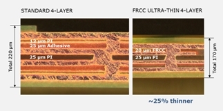
Figure 5. Standard 4-layer flex system vs. ultra-thin 4-layer flex system.
Rigid Systems
For applications that require a 2D PCB, ultra-thin rigid materials are available. These are typically used as packaging substrates for ICs, where they help make the entire component very thin. For example, a 6-layer rigid system using an ultra-thin material is about 260 µm thick, the same system with standard material is 512 microns thick. With the ultra-thin rigid materials, it is possible to achieve pitches smaller than 175 microns, lines or spaces 25 microns wide, via diameters of 50 microns, and pad diameters of 100 microns.
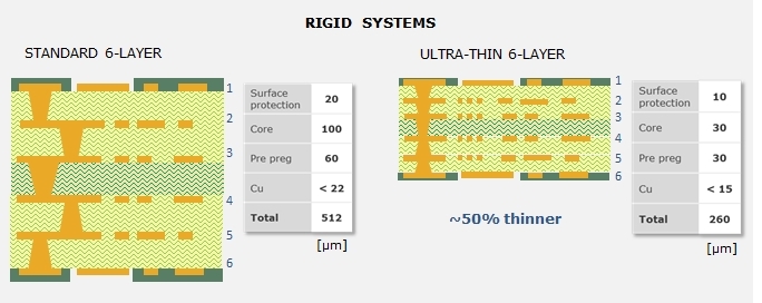
Figure 6. 6-layer stack-up with standard rigid material compared to 6-layer stack-up with ultra-thin base material.
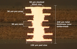
Figure 7. 6-layer rigid stack-up with ultra-thin materials.
The coefficient of thermal expansion of the rigid substrate is one of the most important properties for chip packaging substrates. If it is not matched well with the silicon die, it can lead to cracks that adversely affect packaging production and the assembly of the components onto the substrate. Problems with thermal expansion can even lead to failures during device use. Ultra-thin substrate materials also need to have very good high-frequency properties to achieve the requirements of today’s high-speed telecom applications.
Considerations for Ultra-Thin Materials
Because ultra-thin materials require specific design approaches, fabrication technology, and other considerations, it is critical to use an experienced PCB manufacturer with advanced engineering services.
Advanced techniques such as laser direct imaging can be used with ultra-thin materials, but highly precise registration processes are required because the features are typically smaller when a thinner material is used.
It’s important to note that the thinner material can lead to warpage and increased flexibility, which make proper handling during assembly more critical than with traditional materials. The reduced dimensions and smaller pads require higher accuracy during assembly, and when thinner materials are used, it can also be more difficult to place the finalized circuits into the end application without breaking them. Because of these challenges, it is critical to have early discussions with the PCB manufacturer regarding handling requirements and the number of units within a delivery panel.
The additional handling and fixtures needed with ultra-thin flex materials increase assembly and handling costs. However, lower process and material costs can help balance these. Material costs are reduced as less copper is required. Consulting with the engineering team of the PCB manufacturer during the design phase can help ensure the most cost-effective solution that meets the performance needs of the specific application.
Assuring Quality and Reliability
The reliability of the interconnect structure improves with thinner stack-ups when using ultra-thin materials. Smaller expansion along the Z axis results in less stress for vias during temperature cycles.
Dyconex has created a center of competence for product reliability. This testing laboratory unifies all the processes necessary for precise monitoring of product reliability. The equipment includes stations for electrical fault isolation and thermography as well as multiple interconnect stress test (IST) units, bending testers, a soldering simulation oven, and instruments for thermomechanical and dynamic mechanical analysis (TMA, DMA). Furthermore, a scanning electron microscope and various optical microscopes can be used for investigations.
For critical medical or aerospace applications, the laboratory has developed extensive and systematic methodologies that make it possible to gather solid evidence about product reliability by employing accelerated test procedures such as the IST test. In IST tests, special test coupons that include vias are subjected to temperature cycles, after which they are measured for possible changes in resistance within the test coupon. Any corresponding increase in resistance is indicative of damage.
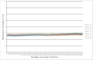
Figure 8. IST test results for multilayer system based on ultra-thin rigid material.
Conclusion
Ultra-thin PCB base materials are suitable for all markets where miniaturization and high reliability play a role. They can enable miniaturization with increased functionality through higher-density designs. Thinner material leads to smaller vias, reduced aspect ratio of vias, smaller lines and spaces, less copper plating, and better fill grades, but it can also increase handling complexity. Working with a PCB manufacturer that offers advanced engineering services can help ensure your design is compact while remaining cost-effective and reliable.
Daniel Schulze has studied at the Technical University of Dresden and holds a diploma in electrical engineering. During his diploma thesis and an internship at the Georgia Tech Packaging Research Center, he got involved with working on optical waveguides embedded in PCBs. In 2005, he began as product engineer at Dyconex AG. Since 2008, he has been an engineering manager at Dyconex and is responsible for the product development of PCBs used in medical imaging, hearing aids, cochlear implants, industrial, and HF applications.
Manufacturers of the printed circuit boards (PCBs) that are at the heart of these electronic devices have been making them more compact and lighter primarily by decreasing the size of the copper features and board materials. Extremely thin base materials are making it possible to take miniaturization beyond what was previously possible without compromising reliability or performance.
Thinner Substrates
Although a great deal of miniaturization can be achieved in the X and Y directions, the technology is beginning to reach its limits. Another level of compactness is possible by using rigid and flexible ultra-thin base materials to make highly reliable PCBs that are thinner. While miniaturization in X / Y direction can greatly reduce the footprint of PCBs, miniaturization in the Z direction leaves more space for other components and reduces the overall thickness of the device.
Figure 1. Evolution of pacemakers. Image courtesy of Dyconex.
With thinner base materials, less plated copper is needed to fill via connections. This automatically results in thinner copper layers and, therefore, lines/spaces with smaller resolutions and a reduced interconnect footprint.
Flex systems
Medical devices, like hearing aids and active implants, often require PCBs that can fit into the smallest area possible to improve the patients’ comfort. With flexible substrates, it is possible to create PCBs that fold to reduce the surface area and volume needed to house the PCB and thus increase the integration density. Using thinner flex materials rather than traditional thick flex materials can reduce the space needed for the PCB even more. For example, a six-layer flex system is about half the thickness of a system fabricated with standard flexible materials.
Figure 2. 6-layer stack-up with standard flex material compared to 6-layer stack-up with ultra-thin base material.
Flex systems are used in hearing aids to ensure all the necessary electrical components can be housed within a package that fits in the ear canal. In this case, the circuit board is assembled flat with the integrated circuits, resistors, and capacitors and then folded to reduce the overall footprint.
Figure 3. From flat substrate to folded package.
Ultra-thin flexible substrates also allow better bending. This means the PCBs can be bent with smaller bend radii to achieve even smaller volumes. A comparison is shown in Table 1. The improved bending makes ultra-thin flexible materials ideal for making cables that require dynamic bending, as in robotic arms.
| Total Thickness | Min Bend Radius | |
| Standard 6-layer | 397 µm | 2.38 mm |
| Ultra-thin 6-layer | 172 µm | 1.03 mm |
Today, the outer layers of a multilayer flex system typically measure 12 µm for the polyimide and 12 µm for the adhesive. The new FRCC material provided by DYCONEX offers 3- or 5-µm thick polyimide outer layers combined with a minimum 17 µm thick adhesive layer.
Figure 4. Cu clad polyimide laminate.
| Thickness (µm) | |
| Copper | 12 |
| Polymide (PI) | 3, 5 |
| Adhesive (Adh) | 17, 20, 25, 28 |
| Properties | Unit | PI | ADH |
| Dielectric constant (1 GHz) | -- | 3.3 | 3.0 |
| Dissipation factor (1 GHz) | -- | 0.01 | 0.019 |
| Surface resistivity | MΩ | 3x10⁸ | 3x10⁸ |
| Volume resistivity | Ω*cm | 1x10⁸ | 1x10⁸ |
| Insulation resistance | MΩ | 1x10³ | 1x10³ |
| Dielectric strength | kV/mil | 2 | n/a |
| Peel strength (initial/aging) | kN/m | 0.8 | 0.8 |
| Youngs modulus | GPa | 80, 580 | 1 |
| CTE (XY) | ppm/K | 25 | 80, 580 |
| CTE (Z) | ppm/K | n/a | 210 |
| Glass transition temp. Tg (DMA) | °C | 320 | 70, 210 |
| Moisture absorption (23°C, 24h) | % | 1.0 | 1.0 |
| Flammability | -- | VTM-0 | VTM-0 |
Figure 5. Standard 4-layer flex system vs. ultra-thin 4-layer flex system.
Rigid Systems
For applications that require a 2D PCB, ultra-thin rigid materials are available. These are typically used as packaging substrates for ICs, where they help make the entire component very thin. For example, a 6-layer rigid system using an ultra-thin material is about 260 µm thick, the same system with standard material is 512 microns thick. With the ultra-thin rigid materials, it is possible to achieve pitches smaller than 175 microns, lines or spaces 25 microns wide, via diameters of 50 microns, and pad diameters of 100 microns.
Figure 6. 6-layer stack-up with standard rigid material compared to 6-layer stack-up with ultra-thin base material.
| Standard Material | Ultra-thin Material | |
| Thickness of rigid 6-layer system | 512 µm | 260 µm |
| Lines / Spaces | 50 – 70 µm | 30 – 50 µm |
| Via diameter | 75 µm | 50 µm |
| Pad diameter | 150 µm | 100 µm |
| Pitch | 250 µm | 175 µm |
Figure 7. 6-layer rigid stack-up with ultra-thin materials.
The coefficient of thermal expansion of the rigid substrate is one of the most important properties for chip packaging substrates. If it is not matched well with the silicon die, it can lead to cracks that adversely affect packaging production and the assembly of the components onto the substrate. Problems with thermal expansion can even lead to failures during device use. Ultra-thin substrate materials also need to have very good high-frequency properties to achieve the requirements of today’s high-speed telecom applications.
| Properties | Unit | Conditions | Value |
| CTE | ppm/°C | XY < Tg | 5-6 |
| CTE | ppm/°C | Z < Tg | 18-22 |
| Tg | °C | DMA | 280-300 |
| Flexural modulus | GPa | 25°C | 32 |
| Dielectric constant | Er | 1 GHz | 4.4 |
| Dielectric constant | Er | 10 GHz | 4.3 |
| Dissipation factor | -- | 1 GHz | 0.006 |
| Dissipation factor | -- | 10 GHz | 0.008 |
| Dielectric strength | kV/mm | ASTM D149 Method A | 103 |
| Moisture absorption | % | 0.3 | |
| Min thickness core | µm | 30 | |
| Min thickness prepreg | µm | 20 |
Considerations for Ultra-Thin Materials
Because ultra-thin materials require specific design approaches, fabrication technology, and other considerations, it is critical to use an experienced PCB manufacturer with advanced engineering services.
Advanced techniques such as laser direct imaging can be used with ultra-thin materials, but highly precise registration processes are required because the features are typically smaller when a thinner material is used.
It’s important to note that the thinner material can lead to warpage and increased flexibility, which make proper handling during assembly more critical than with traditional materials. The reduced dimensions and smaller pads require higher accuracy during assembly, and when thinner materials are used, it can also be more difficult to place the finalized circuits into the end application without breaking them. Because of these challenges, it is critical to have early discussions with the PCB manufacturer regarding handling requirements and the number of units within a delivery panel.
The additional handling and fixtures needed with ultra-thin flex materials increase assembly and handling costs. However, lower process and material costs can help balance these. Material costs are reduced as less copper is required. Consulting with the engineering team of the PCB manufacturer during the design phase can help ensure the most cost-effective solution that meets the performance needs of the specific application.
Assuring Quality and Reliability
The reliability of the interconnect structure improves with thinner stack-ups when using ultra-thin materials. Smaller expansion along the Z axis results in less stress for vias during temperature cycles.
Dyconex has created a center of competence for product reliability. This testing laboratory unifies all the processes necessary for precise monitoring of product reliability. The equipment includes stations for electrical fault isolation and thermography as well as multiple interconnect stress test (IST) units, bending testers, a soldering simulation oven, and instruments for thermomechanical and dynamic mechanical analysis (TMA, DMA). Furthermore, a scanning electron microscope and various optical microscopes can be used for investigations.
For critical medical or aerospace applications, the laboratory has developed extensive and systematic methodologies that make it possible to gather solid evidence about product reliability by employing accelerated test procedures such as the IST test. In IST tests, special test coupons that include vias are subjected to temperature cycles, after which they are measured for possible changes in resistance within the test coupon. Any corresponding increase in resistance is indicative of damage.
Figure 8. IST test results for multilayer system based on ultra-thin rigid material.
Conclusion
Ultra-thin PCB base materials are suitable for all markets where miniaturization and high reliability play a role. They can enable miniaturization with increased functionality through higher-density designs. Thinner material leads to smaller vias, reduced aspect ratio of vias, smaller lines and spaces, less copper plating, and better fill grades, but it can also increase handling complexity. Working with a PCB manufacturer that offers advanced engineering services can help ensure your design is compact while remaining cost-effective and reliable.
Daniel Schulze has studied at the Technical University of Dresden and holds a diploma in electrical engineering. During his diploma thesis and an internship at the Georgia Tech Packaging Research Center, he got involved with working on optical waveguides embedded in PCBs. In 2005, he began as product engineer at Dyconex AG. Since 2008, he has been an engineering manager at Dyconex and is responsible for the product development of PCBs used in medical imaging, hearing aids, cochlear implants, industrial, and HF applications.
